(Created page with "In this level, we need to build a CPU based on the LEG architecture. This is a significant milestone and quite a challenging one (it took me 20 hours to figure it out at the time). File:Leg.png I propose a feasible implementation solution: Firstly, I encapsulated the register group. Below is a component called "WikiRegisterGroup." It's important to note that a modified register is utilized here. File:RegisterPlus.png The above has two input signals. The firs...") |
No edit summary |
||
| (One intermediate revision by one other user not shown) | |||
| Line 10: | Line 10: | ||
The above has two input signals. The first one controls whether the register outputs to the first bus, and the second one controls whether it outputs to the second bus. | The above has two input signals. The first one controls whether the register outputs to the first bus, and the second one controls whether it outputs to the second bus. | ||
[[File:WikiRegisterGroupa-remake.png]] | |||
[[File: | |||
This component also accepts an input called "INPUT," which can be used to write to the corresponding register based on the value of "res." | This component also accepts an input called "INPUT," which can be used to write to the corresponding register based on the value of "res." | ||
Then, the parameters 1 and parameters 2 are decoded, while the program counter and IN/OUT are separately extracted. | Then, the parameters 1 and parameters 2 are decoded, while the program counter and IN/OUT are separately extracted. | ||
[[File: | [[File:WikiRegisterGroupa-remake-decode-arg.png]] | ||
| Line 22: | Line 21: | ||
[[File: | [[File:WikiRegisterGroupa-remake-decode-result.png]] | ||
| Line 49: | Line 48: | ||
Finally, we connect the value of the program counter to the bus. | |||
Finally, we connect the value of the program counter to the bus and enable RegisterGroup and AlU. | |||
[[File:Leg Counter.png]] | [[File:Leg Counter.png]] | ||
Latest revision as of 02:01, 21 March 2024
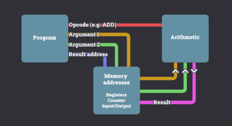
In this level, we need to build a CPU based on the LEG architecture. This is a significant milestone and quite a challenging one (it took me 20 hours to figure it out at the time).
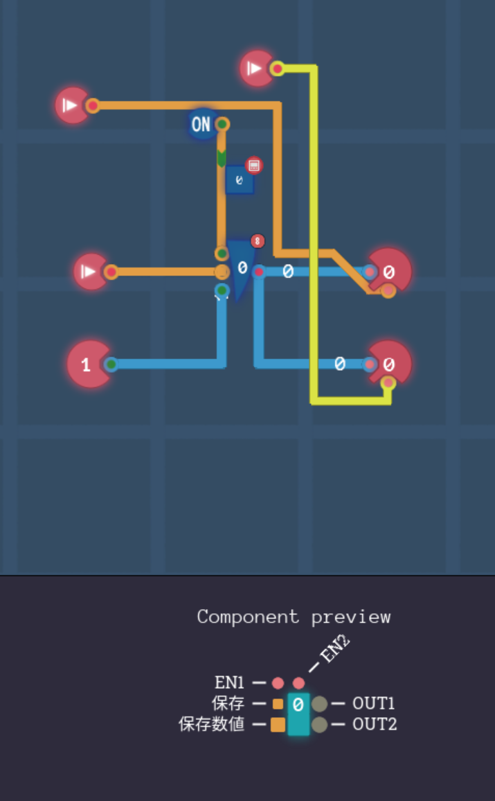
I propose a feasible implementation solution: Firstly, I encapsulated the register group. Below is a component called "WikiRegisterGroup." It's important to note that a modified register is utilized here.
The above has two input signals. The first one controls whether the register outputs to the first bus, and the second one controls whether it outputs to the second bus.
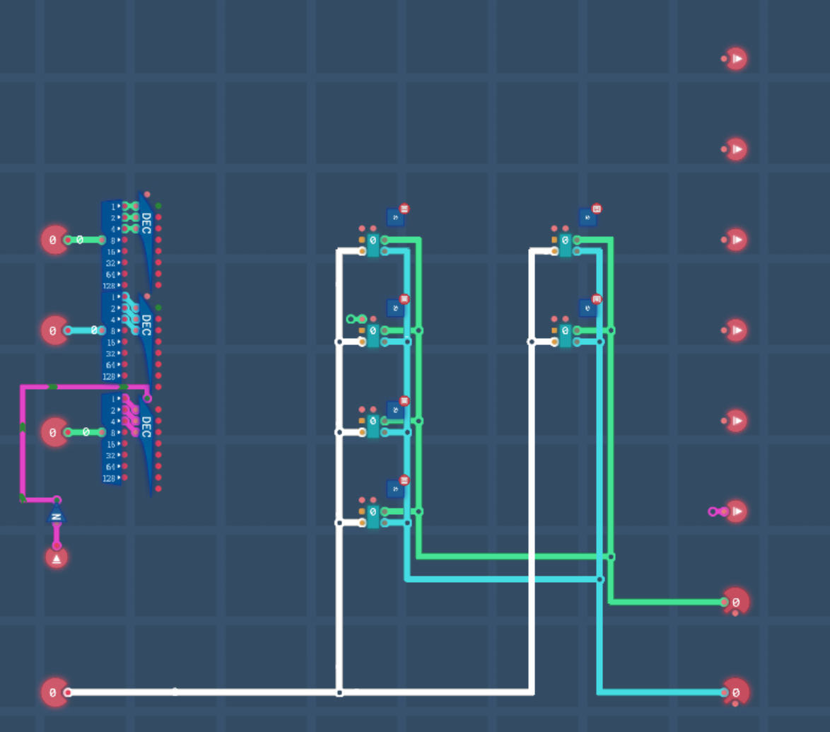
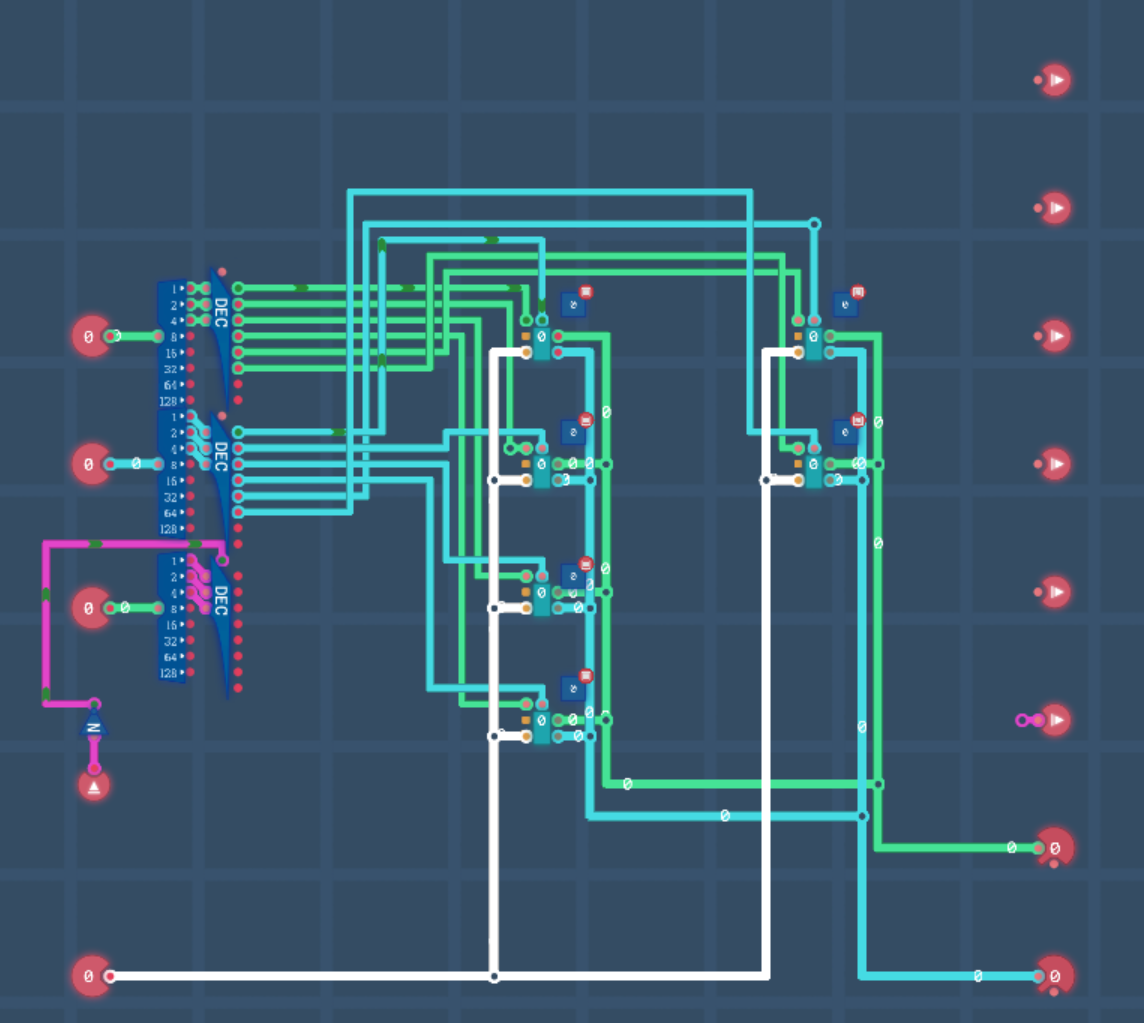
This component also accepts an input called "INPUT," which can be used to write to the corresponding register based on the value of "res." Then, the parameters 1 and parameters 2 are decoded, while the program counter and IN/OUT are separately extracted.
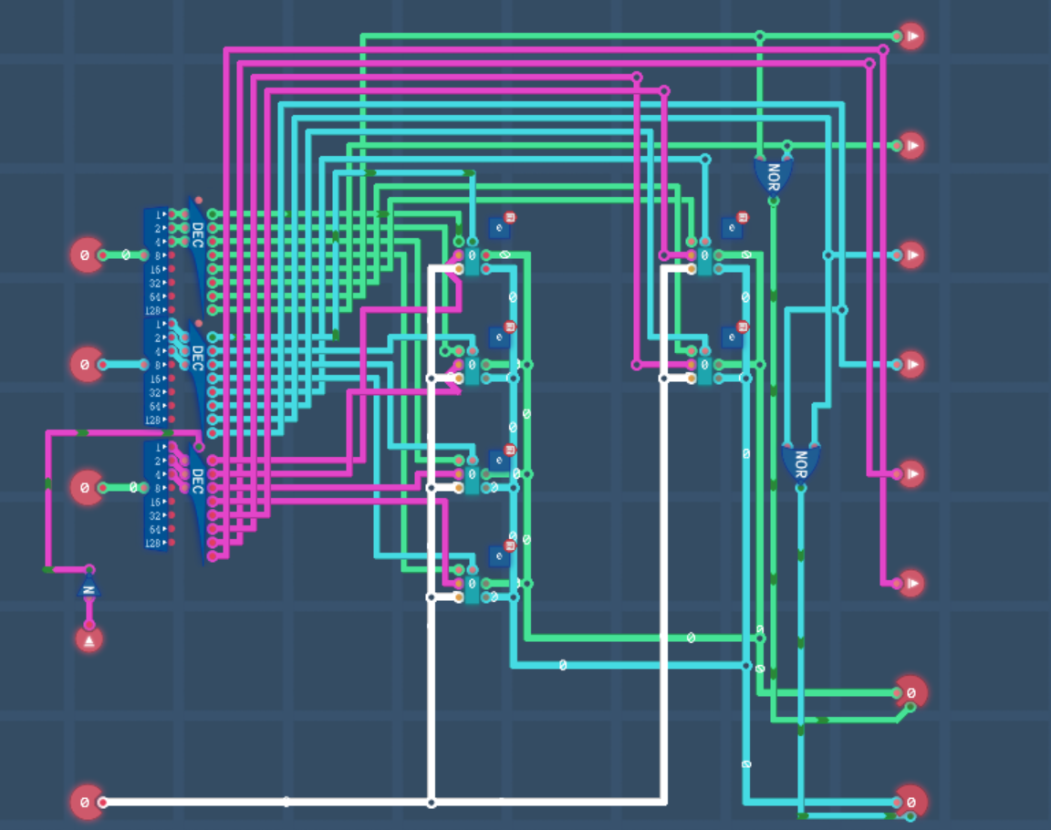
The addresses where the results are stored are also decoded, and the corresponding counters and output pins are printed out.
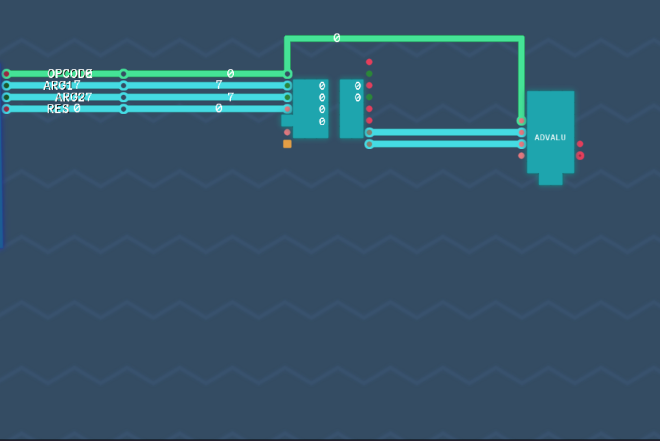
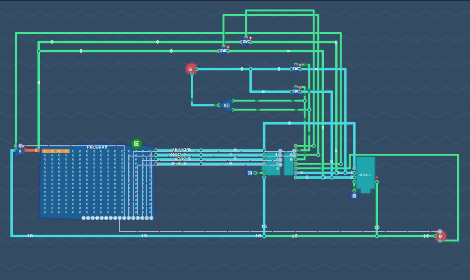
Assuming you have already completed an ALU with addition functionality, let's proceed from the following diagram:
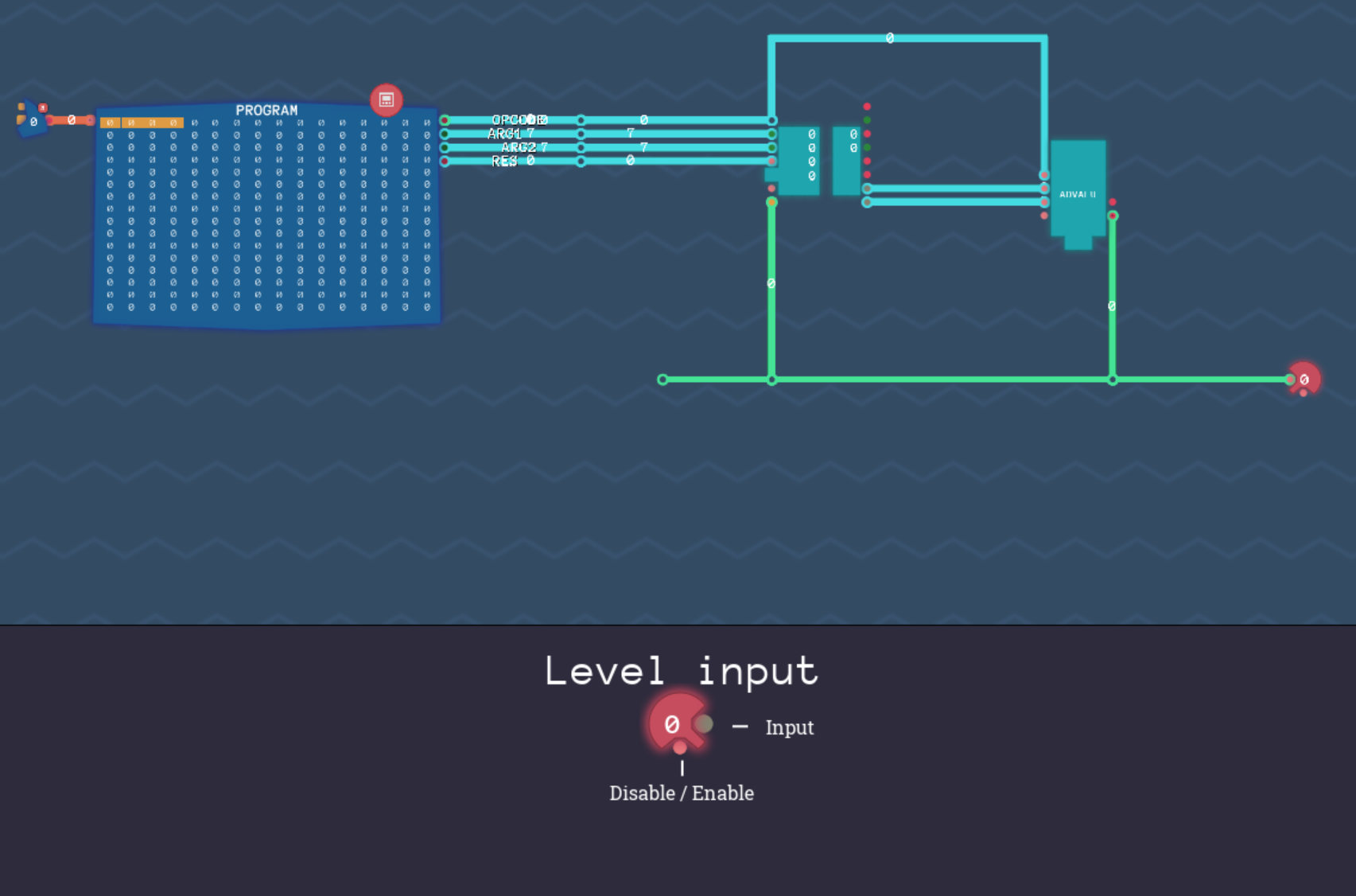
We put the result computed by the ALU onto the bus and connect it to the INPUT input of the register group.
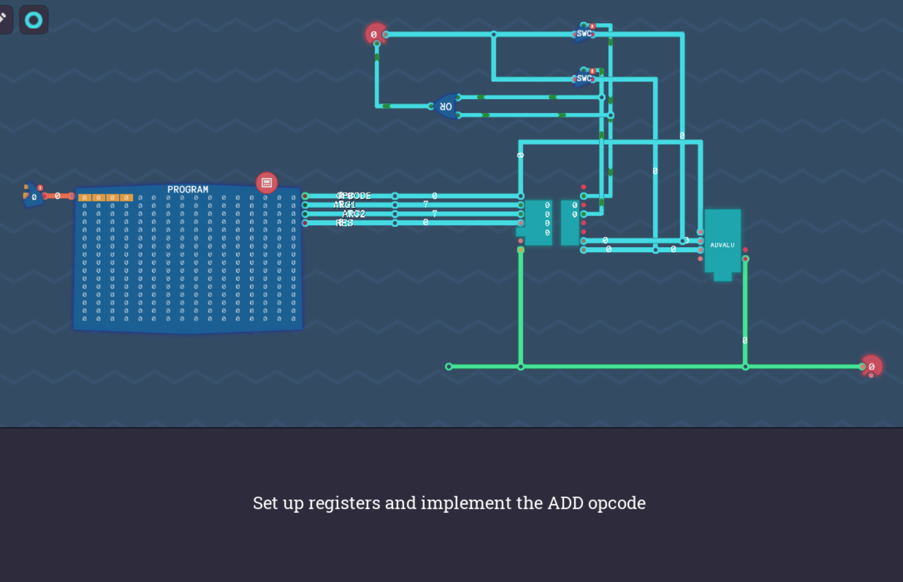
Next, we read the inputs. Since there are two parameters, both of which could be inputs, we use switches connected to the output buses of the two register groups.
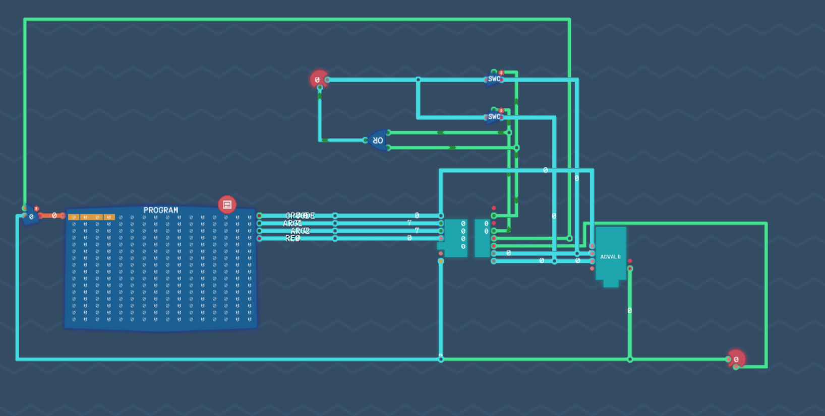
Next, we connect the result (RES) to its corresponding positions (the program counter, output switches).
Finally, we connect the value of the program counter to the bus and enable RegisterGroup and AlU.
